What does the second-level cache frequency mean. Processor cache effects gallery
1) Cache memory
Cache memory (from English cache, literally - "stash", "pod", American English. cash - "cash", "money at hand") - computer memory with quick access, where part of the data from another is duplicated carrier with slower access, or data is stored that require "expensive" (in terms of time) computations. Sometimes, cache memory is referred to simply as "cache" for brevity.The cache memory allows you to access frequently required data faster than it would be without using it. The process of organizing access through the cache memory is called caching, and the memory that is cached is called main memory.
^
RAM caching
Most often, the term cache memory is used to refer to cash-memory between central processing unit (CPU) registers and random access memory (RAM).
The cache memory can provide a significant gain in productivity because currently RAM clock speed significantly less than the CPU clock speed. The clock speed for cache memory is usually not much less than the CPU clock.
^
Cache levels
Separation of cache memory into several levels (up to 3 for general purpose processors as of early 2007). An N + 1 cache is always larger and slower in speed than an N cache.
The fastest memory is the first level cache (aka L1-cache), in fact, it is an integral part of the processor, since it is located on the same crystal and is a part of functional blocks, without it the processor will not be able to function. L1 memory operates at the processor frequency, and in general it can be accessed every clock cycle (it is often possible to perform even several reads / writes simultaneously), access latency is usually 2-4 core clock cycles, the volume of this memory is usually small - no more than 64 KB. The second fastest is L2 (unlike L1, it can be turned off while maintaining the processor's performance), the second-level cache, it is usually located either on the chip, like L1, or in the immediate vicinity of the core, for example, in a processor cartridge (only in slot processors), in older processors it was located on the motherboard. The volume of L2 is larger - from 128 Kb to 1-4 Mb. Typically, the L2 latency of an on-die core is 8 to 20 core clocks. L3 cache is the least responsive and usually located separately from the CPU core, but it can be very impressive in size and still significantly faster than RAM.
^
Cache associativity
One of the fundamental characteristics of cache memory - the level of associativity - reflects its logical segmentation. The fact is that a sequential search of all cache lines in search of the necessary data would require tens of clock cycles and would negate all the gain from using the memory built into the CPU. Therefore, RAM cells are rigidly bound to cache lines (each line can contain data from a fixed set of addresses), which significantly reduces the search time. Each RAM cell can have more than one cache line associated with it: for example, n-way set associative means that information at a certain RAM address can be stored in n cache locations.
For the same cache size, the scheme with the highest associativity will be the least fast but most efficient.
^
Caching write policy
When reading data, the cache memory gives a clear performance benefit. When recording data, the gain can only be obtained at the cost of reducing the reliability. Therefore, different applications may choose one or another cache write policy.
There are two main write cache policies - write-through and write-back.
Write-through means that when the contents of a memory cell change, the write occurs synchronously to both the cache and main memory.
lazy write means that you can postpone the moment of writing data to the main memory, and write them only to the cache. In this case, the data will be unloaded into RAM only if some other device (another CPU, DMA controller) accesses them or if there is not enough space in the cache to accommodate other data. Performance, compared to write-through, increases, but this can jeopardize the integrity of the data in main memory, as a software or hardware failure can prevent data from being overwritten from the cache to main memory. In addition, in the case of RAM caching, when two or more processors are used, it is necessary to ensure the consistency of data in different caches.
External storage caching
Many peripheral storage devices use cache to speed up their work, in particular, hard drives use cache memory from 1 to 16 MB (models supporting NCQ/TCQ use it to store and process requests), CD / DVD / BD drives also cache the read information to speed up re-access.
The operating system also uses part of the RAM as a cache of disk operations (including for external devices that do not have their own cache memory, for example, USB-flash, floppy disk drive).
^
Caching web pages
The process of saving frequently requested documents to intermediate proxy servers or the user's machine, in order to prevent their constant loading from the source server and reduce traffic... Those. moving information closer to the user. Caching is controlled using HTTP headers
^
Caching work results
Many programs write intermediate or auxiliary results of work somewhere, so as not to calculate them every time they are needed. This speeds up the work, but requires additional memory (RAM or disk). An example of such caching is indexing databases.
2) Intel 80286 (also known as i286) - 16- bit x86-compatible second generation Intel processor released 1st of February of the year. This processor is an improved version of the processor Intel 8086 and was 3-6 times faster than him. The processor was used mainly in IBM PC compatible PCs.
Description
The i286 processors were developed in parallel with the processors Intel 80186/ , however, it lacked some of the modules available in the Intel 80186 processor. The i286 processor was produced in the exact same package as the i80186 - LCC, as well as in 68-pin PGA packages. The new processor has increased the number of registers, added new instructions, added a new processor mode - protected mode... The processor had 6 byte queue (like Intel 8086). Address buses and data now they are not multiplexed (that is, addresses and data are transmitted on different legs). The address bus is increased to 24 bits, thus the volume RAM can be 16 MB. The processor did not know how to perform operations on floating point numbers; to perform such operations, a mathematical coprocessor, for example Intel 80287.Registers
11 new registers were added to the 14 registers of the Intel 8086 processor, which are necessary for the implementation of the protected mode and other functions: register machine status word, 16 bits (MSW); task register, 16 bits (TR); registers descriptor table, one 64-bit and two 40-bit (GDTR, IDTR, LDTR) and 6 extension registers of segment registers, 48 bits.Operating modes of the i286 processor
The i286 processor has two modes of operation - protected mode and real mode... In real mode, the processor was fully compatible with previous x86 processors, that is, the processor could execute programs intended for Intel 8086/8088 / 8018x without reassembly or with reassembly with minimal modifications. Only 20 data bus lines took part in the formation of the address, so the maximum amount of addressable memory in this mode remained the same - 1 MB. In protected mode, the processor could address up to 1 GB virtual memory(while the amount of real memory was no more than 16 MB), due to a change in the memory addressing mechanism. Switching from real mode to protected mode is software-based and relatively simple, but the reverse transition requires a hardware reset of the processor, which in IBM PC-compatible machines was usually performed using a keyboard controller. The Machine Status Word (MSW) register is used to track the current processor mode. Real-mode programs without modifications in protected mode cannot be executed, as well as machine BIOS programs.
The physical address is formed as follows. Segment registers store selector containing index descriptor v descriptor table(13 bits), 1 bit defining which descriptor table will be accessed (local or global) and 2 bits of the requested privilege level. Then the corresponding descriptor table and the corresponding descriptor are accessed, which contained the initial, 24-bit, segment address, segment size and access rights. Then the required physical address was calculated by adding the segment address with the offset stored in a 16-bit pointer register.
However, the protected mode in the Intel 80286 processor also had some drawbacks, such as incompatibility with programs written for the real MS-DOS mode; to switch from the protected mode to the real mode, a hardware reset of the processor was required.
^
Protected mode
Memory protection mode. Designed by Digital Equipments (DEC) for VAX-11 32-bit computers. The main idea comes down to the formation of tables of memory descriptions, which determine the state of its individual segments / pages, etc. If there is not enough memory, the operating system can unload part of the data from the main memory to disk, and add an indication to the description table that this data is not in memory. When trying to access missing data, the processor will generate an exception (a kind of interrupt) and give control to the operating system, which will return the data to memory and then return control to the program. Thus, for programs, the process of swapping data from disks is imperceptible.
The memory protection mechanism is also used in processors from other manufacturers.
Real mode (or real address mode) - this name was given to the previous method memory addressing after the appearance 286th processor supporting protected mode.
^
Technical description
With this way of organizing memory, the content register the segment pointer was multiplied by 16, that is, shifted to the left by 4 bit and summed up with the pointer. That is, addresses 0400h: 0000h and 0000h: 4000h refer to the same address, since 400h * 16 = 4000h. This method allowed addressing 1 MB + 64 KB - 16 bytes of memory, but due to the presence of only 20 address lines in early processors, only 1 MB was addressed.
Usage
In this mode, processors worked only in older versions DOS... Additional memory beyond 1 MB could not be addressed in real mode. Subsequently, independent programmers found a way to work around this limitation. Despite the fact that the firm Intel did not provide for the return of the 80286 processor from protected to real mode, a way to reboot it was found. After such a reboot, the ability to access the upper memory blocks remained. Subsequently 386 processors allowed to perform similar actions without tweaks and the himem driver performing these actions was introduced into the operating system MS DOS... In the future, this led to incompatibility of some programs.Then they began to leave the real mode with the help of protected mode managers working in the DOS environment, such as: rtm, dpmi, DOS16M, DOS4G, DOS4GW. Some of which even allowed the use of virtual memory in the DOS environment by enabling special control variables (for example: DOS4GVM = ON).
Subsequently, to completely abandon real mode, another special mode of virtual addresses V86 was introduced into protected mode. In this case, programs are able to use the previous method of calculating a linear address without leaving the protected mode of the processor. This mode made it possible to organize the work of the old DOS system inside the new multitasking systems. Microsoft Windows.
Virtual mode
In addition to the real and protected mode of operation, the i80386 and i80486 processors provide the 8086 virtual processor mode (virtual mode), which the processor can enter from the protected mode. Virtual mode allows you to emulate the i8086 processor while in protected mode. This, in particular, makes it possible in a multitasking operating system to organize the simultaneous execution of several programs focused on the i8086 processor.
^
3) Dual independent bus architecture
Architecture constructing processor, in which data is transmitted over two tires independently of each other, simultaneously and in parallel.
Relieves many problems bandwidth computer platforms, was developed by Intel to satisfy requests application programs, as well as to ensure the possibility of further development of new generations of processors.
The presence of two independent buses allows the processor to access data transmitted on any of the buses simultaneously and in parallel, in contrast to the sequential mechanism characteristic of systems with one bus.
Mechanism of work
The dual independent bus architecture uses two buses: "bus cache 2nd level (L2) (512 KB) "and" system bus "- from the processor to the main memory.
Dual independent bus architecture, for example, more than 3 times faster processor's L2 cache Pentium II with clock frequency 400 MHz vs. processor L2 cache Pentium... As the clock speeds of Pentium II processors increase, the speed of access to the L2 cache will also increase.
Conveyor system bus provides multiple interactions at the same time, increasing the flow information in the system and significantly increasing the overall performance.
Yard tournament:
1. The clock frequency is measured in: GHz
2. Hypertext is: The text in which the transition can be carried out on the selected labels
3. The rewritable laser discs are named: DVD-RW
4. The printer is intended for: Outputting information on paper
5. The program is called the archiver: The program for compressing files
6. Computer performance depends on: CPU clock speed
7. Computer viruses: Created by humans specifically to damage PCs
8. The smallest unit of information is: bit
9. Hard drives were named: Winchester
10. To connect the computer to the telephone network, use: Modem
11. How many bits are contained in one byte: 8
12. Select the correct ascending order: Byte, Kilobyte, Megabyte, Gigabyte
13. For long-term storage of information is used: Hard disk
14. What program is required for installation on a computer: Operating system
15. Processors differ among themselves: Bit depth and clock frequency
City Tournament:
1. The system time of the computer is constantly resetting, how to solve the problem: Replace the BIOS battery
2. Which type of cable is most susceptible to electronic interference: Unshielded twisted pair
3. Which of the listed IP addresses is correct in terms of the format: 192.168.0.3
4. What is a browser: A program for viewing Internet pages
5. Which of the devices does not belong to HID devices: Processor
6. Specify the fastest cache type in the processor: L1
7. What device must be introduced into the network to filter traffic at the border between the external and internal local networks, passing only allowed packets: Firewall
8. The amount of information in DVD: 4.7 GB
9. Graphics in the form of a set of points is called: Raster
10. There is a 25-pin male connector on the back of the computer. What is it: COM port
11. Twisted pair, coaxial, fiber optic are: Cables used to create a network
12. Which of the following happens when using RAID arrays: Increases the reliability of data storage
13. A computer connected to the Internet must have: IP address
14. Which file system is intended for optical media: UDF
15. The elementary object used in the raster graphics editor is: Pixel
Regional tournament:
1. What network protocol does the ping utility use to work: ICMP
2. What protocol checks the correspondence of ip-addresses to mac-addresses: ARP
3. For what purposes is the DNS system: To obtain information about domains
4. Which of the following parameters the client cannot receive from the DHCP server: IP address of the SMTP server
5. What port number is officially allocated by IANA for SMTP protocol: 25
6. What technology is provided specifically in case of server hard disk failure: RAID
7. What type of attack is carried out to intercept packets: Sniffing
8. Which utility should you use to scan IP networks: nmap
9. Which of the following protocols implements guaranteed delivery of information packets: TCP
10. Which Windows XP command allows you to display the routing table: route
11. What protocol is not an email protocol: HTTP
12. Which of the following protocols implements not guaranteed delivery of information packets: IP protocol
13. Which Windows command can be used to check for the presence of a TCP server on an arbitrary port of a remote computer: telnet
14. At what level of the OSI network model does the router operate:
15. Which of the following tools is used to diagnose server vulnerabilities: XSpider scanner
Federal tournament:
1. In ANSI / SQL, which operator allows you to combine the results of several queries, without excluding the same lines: union
2. What type of server will allow organizing the general access of several workstations to the Internet: Proxy server
3. HTML. What the tag's colspan attribute defines: Concatenates cells horizontally
4. In ANSI / SQL, which of the following logical orders of execution of the select statement is correct: from -> where -> group by -> join
5. HTML. Which tag should be used to display text with all spaces:
6. In ANSI / SQL, which of the following restrictions in the create table command determines the value that is automatically set when a record is added, if the user does not enter it: default
7. Which Windows command allows you to get a list of TCP connections: netstat-a
8. HTML. Which tag is not a tag parameter : href
9. HTML. Which spelling of the given options is correct:
10. HTML. Which of the following code snippets right-aligns the contents of the cell:
11. HTML. Which tag defines the background image: body background
12. HTML. Which tag is a line feed tag:
13. In ANSI / SQL, which of the following query keywords is used to sort in descending order: desc
14. HTML. Which line contains the correct syntax: body (color: black)
15. HTML. Which tag is not a list organization tag:International tournament:
1. What is the catch keyword in C ++: Exception handling block
2. Java. Which of the following fractional literal declarations is not correct: double d = 1e0;
3.C ++. The scope of a variable declared inside a block extends: From the place of the variable declaration to the end of the block
4. Java. What modifier should be applied so that some fields of the object are not serialized by the appropriate mechanism by default: transient
5. Java. What is the difference between the break and continue statements: continue can only be used inside a loop
6. Which of the following is a C ++ declaration: int * a
7. What's in the ANSI / SQL select statement allows you to select all field names from a list of tables: *
8. Java. What is the result of executing the specified string: int i = Integer.MAX_VALUE + 10: The value of i will become a negative number
9. Java. Which of the following code snippets will lead to a compilation error due to incorrect use of comments: circle.get / * comment * / Radius ();
10. In C ++, the typeid () operator returns: A reference to the type of the standard library called type_info
11. How does the context resolution operation (scope resolution operation) look like in C ++: ::
12. How classes differ from structures in C ++: By default access modifier to fields and member functions
13. In ANSI / SQL, which keyword is used to create an alias for a column of a selection result: ALIAS
14. What is the sizeof operator for in C ++: To determine the number of bytes occupied by a type
15. How to call this function correctly in C ++: int sum (int a, int b) (return a + b): sum (7,8);
- Translation
Almost all developers know that the processor cache is such a small but fast memory that stores data from recently visited memory regions - the definition is short and rather accurate. However, knowing the boring details of how the cache works is necessary to understand the factors that affect the performance of your code.
In this article, we will look at a number of examples that illustrate the various features of caches and their impact on performance. The examples will be in C #, the choice of language and platform does not so much affect the performance assessment and final conclusions. Naturally, within reasonable limits, if you choose a language in which reading a value from an array is equivalent to accessing a hash table, you will not get any interpretable results. Translator's notes are in italics.
Habracut - - -
Example 1: memory access and performance
How much faster do you think the second cycle is?int arr = new int;// first
for (int i = 0; i< arr.Length; i++) arr[i] *= 3;// second
for (int i = 0; i< arr.Length; i += 16) arr[i] *= 3;
The first loop multiplies all the values in the array by 3, the second loop only multiplies every sixteenth value. The second cycle makes only 6% work the first cycle, but on modern machines, both cycles are executed in approximately the same time: 80 ms and 78 ms respectively (on my machine).The answer is simple - memory access. The speed of these loops is primarily determined by the speed of the memory subsystem, and not by the speed of integer multiplication. As we will see in the next example, the number of calls to RAM is the same in the first and second cases.
Example 2: the impact of cache lines
Let's dig deeper - let's try other step values, not only 1 and 16:for (int i = 0; i< arr.Length; i += K /* шаг */ ) arr[i] *= 3;
Here is the running time of this cycle for various values of the step K:
Please note that when the step values are from 1 to 16, the running time practically does not change. But with values greater than 16, the running time is approximately halved every time we double the step. This does not mean that the loop magically starts to work faster, it just decreases the number of iterations. The key point is the same run time with step values from 1 to 16.
The reason for this is that modern processors do not access memory byte-by-byte, but in small blocks called cache lines. Typically, a string is 64 bytes in size. Whenever you read a value from memory, at least one cache line goes into the cache. Subsequent access to any value from this line is very fast.
Due to the fact that 16 int values take up 64 bytes, loops with steps from 1 to 16 access the same number of cache lines, more precisely, all cache lines of the array. At step 32, every second line is accessed, at step 64, every fourth line is accessed.
Understanding this is very important for some optimization techniques. The number of calls to it depends on the location of the data in memory. For example, unaligned data may require two calls to RAM instead of one. As we found out above, the speed of work will be two times lower.
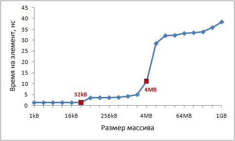
Example 3: Sizes of the first and second level caches (L1 and L2)
Modern processors typically have two or three levels of caches, commonly referred to as L1, L2, and L3. You can use the CoreInfo utility or the GetLogicalProcessorInfo Windows API function to find out the sizes of caches at different levels. Both methods also provide information about the size of the cache line for each level.On my machine, CoreInfo reports 32KB L1 data caches, 32KB L1 instruction caches, and 4MB L2 data caches. Each core has its own personal L1 caches, L2 caches are common for each pair of cores:
Logical Processor to Cache Map: * --- Data Cache 0, Level 1, 32 KB, Assoc 8, LineSize 64 * --- Instruction Cache 0, Level 1, 32 KB, Assoc 8, LineSize 64 - * - Data Cache 1, Level 1, 32 KB, Assoc 8, LineSize 64 - * - Instruction Cache 1, Level 1, 32 KB, Assoc 8, LineSize 64 ** - Unified Cache 0, Level 2, 4 MB, Assoc 16, LineSize 64 - * - Data Cache 2, Level 1, 32 KB, Assoc 8, LineSize 64 - * - Instruction Cache 2, Level 1, 32 KB, Assoc 8, LineSize 64 --- * Data Cache 3, Level 1, 32 KB, Assoc 8, LineSize 64 --- * Instruction Cache 3, Level 1, 32 KB, Assoc 8, LineSize 64 - ** Unified Cache 1, Level 2, 4 MB, Assoc 16, LineSize 64
Let's check this information experimentally. To do this, let's go through our array, incrementing every 16th value - an easy way to change the data in each cache line. Upon reaching the end, we return to the beginning. Let's check the various sizes of the array, we should see a drop in performance when the array ceases to fit into caches of different levels.The code is like this:
int steps = 64 * 1024 * 1024; // number of iterations
int lengthMod = arr.Length - 1; // array size - power of twofor (int i = 0; i< steps; i++)
{
// x & lengthMod = x% arr.Length, for powers of two
arr [(i * 16) & lengthMod] ++;
}
Test results:
On my machine, performance drops are noticeable after 32 KB and 4 MB - these are the sizes of the L1 and L2 caches.
Example 4: instruction parallelism
Now let's take a look at something else. In your opinion, which of these two loops will run faster?int steps = 256 * 1024 * 1024;
int a = new int;// first
for (int i = 0; i< steps; i++) { a++; a++; }// second
for (int i = 0; i< steps; i++) { a++; a++; }
It turns out that the second loop is almost twice as fast, at least on all the machines I've tested. Why? Because the commands inside the loops have different data dependencies. The first commands have the following dependency chain:In the second cycle, the dependencies are:
The functional parts of modern processors are capable of performing a certain number of certain operations simultaneously, as a rule, not a very large number. For example, it is possible to access data from the L1 cache in parallel at two addresses, it is also possible to simultaneously execute two simple arithmetic instructions. In the first cycle, the processor cannot use these capabilities, but it can in the second.
Example 5: cache associativity
One of the key questions that must be answered when designing a cache is whether data from a certain memory area can be stored in any cache cells or only in some of them. Three possible solutions:Direct mapping caches are prone to conflicts, for example, when two rows compete for one cell, alternately pushing each other out of the cache, the efficiency is very low. On the other hand, fully associative caches, while free from this drawback, are very complex and expensive to implement. Partially associative caches are a typical trade-off between implementation complexity and efficiency.
- Direct mapping cache, the data for each cache line in RAM is stored in only one predefined cache location. The simplest way to compute a mapping is: row_index_in_memory% # of cache_sites. Two rows mapped to the same cell cannot be in the cache at the same time.
- N-input partially-associative cache, each line can be stored in N different cache locations. For example, in a 16-way cache, a row can be stored in one of the 16 cells that make up a group. Typically, strings with equal LSBs share the same group.
- Fully associative cache, any line can be saved to any location in the cache. The solution is equivalent to a hash table in its behavior.
For example, on my machine, the 4MB L2 cache is a 16-way partially-associative cache. All RAM is divided into sets of lines according to the least significant bits of their indices, lines from each set compete for one group of 16 L2 cache cells.
Since the L2 cache has 65,536 cells (4 * 2 20/64) and each group consists of 16 cells, we have 4,096 groups in total. Thus, the least significant 12 bits of the row index determine which group the row belongs to (2 12 = 4096). As a result, lines with addresses divisible by 262,144 (4,096 * 64) share the same group of 16 cells and compete for a place in it.
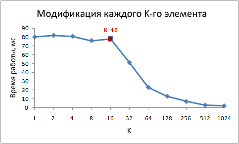
In order for the associativity effects to manifest themselves, we need to constantly access a large number of lines from the same group, for example, using the following code:
public static long UpdateEveryKthByte (byte arr, int K)
{
const int rep = 1024 * 1024; // number of iterationsStopwatch sw = Stopwatch.StartNew ();
int p = 0;
for (int i = 0; i< rep; i++)
{
arr [p] ++;P + = K; if (p> = arr.Length) p = 0;
}Sw.Stop ();
return sw.ElapsedMilliseconds;
}
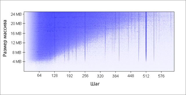
The method increments every K-th element of the array. Upon reaching the end, start over. After a fairly large number of iterations (2 20), we stop. I did runs for different array sizes and K step values. Results (blue - long run time, white - short):
The blue areas correspond to those cases where, with a constant change in data, the cache is not able to accommodate all required data at the same time... The bright blue color indicates the operating time of the order of 80 ms, almost white - 10 ms.
Let's deal with the blue areas:
The detected effects persist even at large values of the parameters:
- Why are vertical lines appearing? The vertical lines correspond to the step values at which too many lines (more than 16) from the same group are accessed. For such values, my machine's 16-way cache cannot accommodate all the required data.
Some of the bad strides are powers of two: 256 and 512. For example, consider stride 512 and an 8MB array. At this step, there are 32 sections in the array (8 * 2 20/262 144), which are fighting with each other for cells in 512 cache groups (262 144/512). The area is 32, and there are only 16 cells in the cache for each group, so there is not enough space for all.
Other step values, which are not powers of two, are simply unlucky, which causes a large number of calls to the same cache groups, as well as leads to the appearance of vertical blue lines in the figure. At this point, fans of number theory are invited to ponder.
- Why do vertical lines break off at the 4MB border? When the array size is 4 MB or less, the 16-way cache behaves like a fully associative cache, that is, it can accommodate all the data in the array without conflicts. There are no more than 16 areas fighting for one cache group (262 144 * 16 = 4 * 2 20 = 4 MB).
- Why is there a big blue triangle on the top left? Because with a small step and a large array, the cache is not able to accommodate all the necessary data. The degree of cache associativity plays a minor role here, the limitation is related to the size of the L2 cache.
For example, with an array size of 16MB and a step of 128, we access every 128th byte, thus modifying every other line in the array cache. It takes 8 MB to store every other line in the cache, but I only have 4 MB on my machine.
Even if the cache were fully associative, it would not be able to store 8 MB of data in it. Note that in the example already considered with a step of 512 and an array size of 8 MB, we only need 1 MB of cache to store all the data we need, but this cannot be done due to insufficient cache associativity.
- Why is the left side of the triangle gradually gaining in intensity? The maximum intensity occurs at a step value of 64 bytes, which is equal to the size of the cache line. As we saw in the first and second examples, sequential access to the same row costs almost nothing. Let's say in a 16 byte step, we have four memory accesses for the price of one.
Since the number of iterations is equal in our test for any step value, a cheaper step results in less running time.
Cache associativity is an interesting thing that can manifest itself under certain conditions. Unlike the rest of the issues discussed in this article, it is not so serious. This is definitely not something that requires constant attention when writing programs.
Example 6: False Cache Split
On multi-core machines, another problem can be encountered - cache alignment. Processor cores have partially or completely separate caches. On my machine, the L1 caches are separate (as usual) and there are two L2 caches shared by each pair of cores. The details may vary, but in general, modern multi-core processors have tiered hierarchical caches. Moreover, the fastest, but also the smallest caches belong to individual cores.When one of the cores modifies a value in its cache, the other cores can no longer use the old value. The value in the caches of other kernels must be updated. Moreover, it needs to be updated completely the entire cache line because caches operate on row-level data.
Let's demonstrate this problem with the following code:
private static int s_counter = new int;private void UpdateCounter (int position)
{
for (int j = 0; j< 100000000; j++)
{
s_counter = s_counter + 3;
}
}
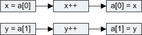
If on my four-core machine I call this method with parameters 0, 1, 2, 3 simultaneously from four threads, then the running time will be 4.3 seconds... But if I call the method with parameters 16, 32, 48, 64, then the running time will be only 0.28 seconds.Why? In the first case, all four values processed by threads at any given time are likely to fall into the same cache line. Each time when one core increases the next value, it marks the cache cells containing this value in other cores as invalid. After this operation, all other kernels will have to cache the line again. This makes the caching mechanism unusable, killing performance.
Example 7: hardware complexity
Even now, when the principles of caches are no secret to you, the hardware will still surprise you. Processors differ from each other in optimization methods, heuristics, and other implementation subtleties.The L1 cache of some processors can access two cells in parallel if they belong to different groups, but if they belong to one, only sequentially. As far as I know, some can even access different quarters of the same cell in parallel.
Processors can surprise you with clever optimizations. For example, the code from the previous example about spurious cache sharing does not work as intended on my home computer - in the simplest cases, the processor can optimize performance and reduce negative effects. If you modify the code a little, everything falls into place.
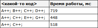
Here's another example of the strange quirks of iron:
private static int A, B, C, D, E, F, G;private static void Weirdness ()
{
for (int i = 0; i< 200000000; i++)
{
<какой-то код>
}
}
If instead of<какой-то код>substitute three different options, you can get the following results:
Incrementing fields A, B, C, D takes longer than incrementing fields A, C, E, G. What's even weirder, incrementing fields A and C takes longer than fields A, C and E, G. I don't know exactly what the reasons for this are, but perhaps they are related to memory banks ( yes, yes, with the usual three-liter memory savings banks, not what you thought). Those who have ideas on this matter, please express themselves in the comments.
On my machine, the above is not observed, nevertheless, sometimes there are abnormally bad results - most likely, the task scheduler makes its own "adjustments".
The lesson learned from this example is that it is very difficult to fully predict the behavior of hardware. Yes, can predict a lot, but you need to constantly confirm your predictions through measurements and testing.
Conclusion
I hope that all of the above has helped you understand the structure of processor caches. Now you can put this knowledge into practice to optimize your code.


 Character overview and tests punishing baraka mortal kombat x
 The best arcade racing games for pc
 What does the constellation Orion look like?
 Satellite map of the earth Satellite map of America online